ADN8810
Rev. A | Page 7 of 16
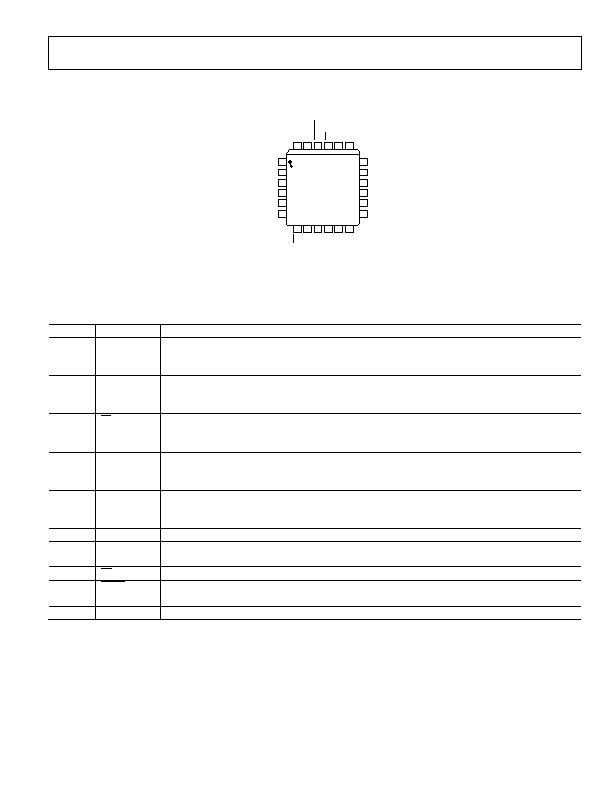
PIN CONFIGURATION AND FUNCTION DESCRIPTIONS
DVSS
NC
AVSS
AVDD
VREF
NC
18
17
16
15
14
13
PIN 1
IDENTIFIER
TOP VIEW
(Not to Scale)
24
ADDR2
RSN
FB
ADDR1
ADDR0
FAULT
C = NO CONNECT
ADN8810
23 22 21 20 19
7 8 9 10 11 12
1
2
3
4
5
6
Figure 3. Pin Configuration
Table 4. Pin Function Description
Pin No.
Mnemonic
Type
Description
1
ADDR2
Digital Input
Chip Address, Bit 2
2
RSN
Analog Input
Sense Resistor RS2 Feedback
3
FB
Analog Input
Sense Resistor RS1 Feedback
4
ADDR1
Digital Input
Chip Address, Bit 1
5
ADDR0
Digital Input
Chip Address, Bit 0
6
FAULT
Digital Output
Load Open/Short Indication
7
SB
Digital Input
Active Deactivates Output Stage (High Output Impedance State)
8, 11
PVDD
Power
Power Supply for IOUT (3.3 V Recommended)
9, 10
IOUT
Analog Output
Current Output
12
ENCOMP
Digital Input
Connect to AVSS
13
NC
No Connection
14
VREF
Analog Input
Input for High Accuracy External Reference Voltage (ADR292ER)
15
AVDD
Power
Power Supply for DAC
16
AVSS
Ground
Connect to Analog Ground or Most Negative Potential in Dual-Supply Applications
17
NC
No Connection
18
DVSS
Ground
Connect to Digital Ground or Most Negative Potential in Dual-Supply Applications
19
SDI
Digital Input
Serial Data Input
20
SCLK
Digital Input
Serial Clock Input
21
CS
Digital Input
Chip Select; Active Low
22
RESET
Digital Input
Asynchronous Reset to Return DAC Output to Code Zero; Active Low
23
DVDD
Power
Power Supply for Digital Interface
24
DGND
Ground
Digital Ground
发布紧急采购,3分钟左右您将得到回复。
相关PDF资料
ADP2140ACPZ3328R7
IC REG DL BCK/LINEAR 10LFCSP
ADP5022ACBZ-6-R7
IC REG TRPL BCK/LINEAR 16WLCSP
ADP5041ACPZ-1-R7
IC REG TRPL BCK/LINEAR 20-LFCSP
ADP5042ACPZ-2-R7
IC REG TRPL BCK/LINEAR 20LFCSP
ADT6402SRJZ-RL7
IC TEMP SENS TRIP PT PP SOT-23-6
ADT6501SRJZP085RL7
IC TEMP SENSOR MICROPWR SOT23-5
ADT7302ARTZ-500RL7
IC SENSOR TEMP 13BIT DGT SOT23-6
ADT7310TRZ
IC TEMP SENSOR 16BIT SPI 8SOIC
相关代理商/技术参数
ADN8810-EVAL
制造商:Analog Devices 功能描述:- Bulk
ADN8810XCP
制造商:Analog Devices 功能描述:- Bulk
ADN8820
制造商:Analog Devices 功能描述:LASER DRVR 1CH 48LFCSP - Trays
ADN8820ACP
制造商:Analog Devices 功能描述:LASER DRVR 1CH 48LFCSP - Bulk
ADN8820-REEL7
制造商:AD 制造商全称:Analog Devices 功能描述:EDFA and CW Laser Controller
ADN8830
制造商:AD 制造商全称:Analog Devices 功能描述:Thermoelectric Cooler Controller
ADN8830ACP
制造商:Analog Devices 功能描述:Temp Sensor Digital 32-Pin LFCSP EP 制造商:Rochester Electronics LLC 功能描述:HIGH PRECISION/EFFICIENCY TEC CONTROLLER - Bulk
ADN8830ACP-REEL
制造商:Analog Devices 功能描述:Temp Sensor Digital 32-Pin LFCSP EP T/R
